AD/DA Converter Module PCF8591
In stock
موديل تحويل Analog الى Digital (تحويل الاشارة التمائلية الى رقمية) يحتوي على اربعة قنوات ومخرج DAC لتحويل الاشارة الرقمية الى تماثلية ويمكن التحكم والاتصال به مباشرة على طريق الاردوينو او متحكم اخر مع كافة امكانيات التحكم
4,750 د.ع
In stock
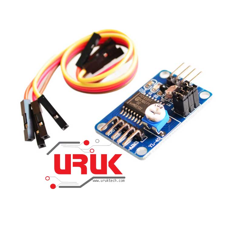
AD/DA Converter Module PCF8591 with 4pin Female-Female Cable
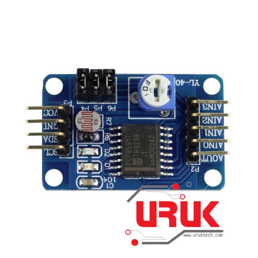
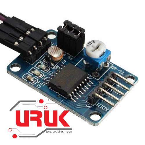
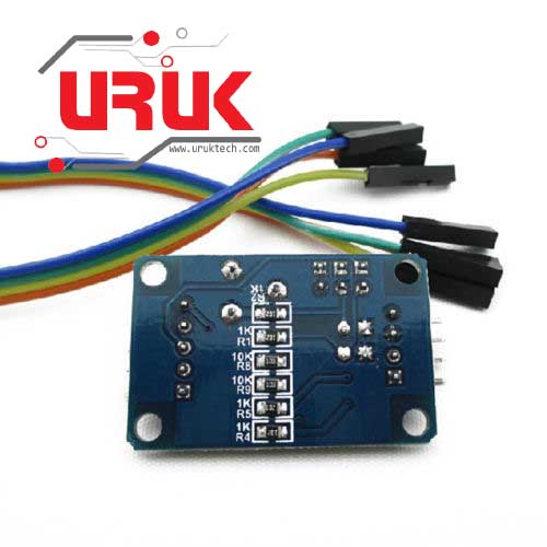
AD/DA converter module based on programmable monolithic chip PCF8591 from NXP, it communicates via I2C. 4 AD inputs, 1 DA output. No speed limit for the I2C bus. A0 A1 and A2 pin can be programmed hardware addresse and thus use up to 8 PCF8591 I2C modules on the same bus. The module also offers a photo resistor (LDR), a thermistor, a single-turn trimmer and two diodes (DA output and VCC presence). Three red jumpers linkq the LDR, the thermistor, trimmer and AD inputs, remove them to use inputs in with another source . this module is shipped in a sealed antistatic bag as most our modules and is provided with Dupont line 4P FF in a row.
Features:
– A module chip using PCF8951
– The module supports external voltage input capture (input voltage range 0-5v)
– Three modules integrated photoresistor acquisition environment through the AD intensity accurate numerical
– The module integrated thermistor, can capture the precise value of the ambient temperature through the AD
– The five-module integrated 1 channel 0-5V voltage input acquisition (blue potentiometer to adjust the input -voltage)
– Module with power indicator light (on the module after power indicator lights)
– The modules with the DA output indicator light board DA output indicator module DA output interface voltage reaches a certain value, the voltage the greater the light brightness is more obvious;
– The module PCB size: 3.6cm * 2.3cm
– Standard double-sided, plate thickness 1.6mm, the layout is nice, surrounded by the through-hole, aperture: 3mm, convenient fixed
Interface:
The module’s left and right, respectively, the external expansion of 2-way pin interface, respectively, as follows:
– Output interface of the left the AOUT chip DA
– The AINO chip analog input interface.
– AIN1 chip analog input interface
– AIN2 chip analog input interface
– AIN3 chip analog input interface
– The right side of the SCL IIC clock interface to access the microcontroller IO port
– The SDA IIC digital interface connected microcontroller IO port
– GND module to an external
– VCC power supply interface external 3.3v-5v
– Module red jumper instructions for use
– Module three red short circuit cap, respectively, the role are as follows:
– P4 connected to the P4 jumper, select thermistor access circuit
– P5 connected to P5 jumper to select the photoresistor access circuit
– P6 connected to the P6 jumper, to select 0-5V adjustable voltage access circuit
Package List:
1 x AD/DA Converter Module
2 x 4Pin Female-Female Cable
- Operating supply voltage 2.5 V to 6.0 V
- Low standby current
- Serial input and output via I2C-bus
- I2C address selection by 3 hardware address pins
- Max sampling rate given by I2C-bus speed
- 4 analog inputs configurable as single ended or differential inputs
- Auto-incremented channel selection
- Analog voltage range from VSS to VDD
- On-chip track and hold circuit
- 8-bit successive approximation A/D conversion
- Multiplying DAC with one analog output.
Based on 0 reviews
Only logged in customers who have purchased this product may leave a review.















There are no reviews yet.